


With the proliferation of wireless devices, nowadays a strong signal strength and high-quality RF antenna design and integration is desired in the devices to allow for optimum performance. Whether it is an off-the shelf-product or a highly customized solution, antenna integration is not trivial and should not be an afterthought. It is a requisite to match the antenna input impedance to 50Ω which ensures maximum power transfer to the antenna from the RF circuitry without any reflections.
Key Implementation Aspects of RF Antenna
One of the most critical factors in the implementation of a trace or a chip antenna is the impedance matching of the antenna to the radio chip. The antenna must be impedance matched when assembled in the product since having an unmatched antenna may result in the following consequences:
- Reduction in Loss of Range: Impedance mismatch causes more signal reflections thereby providing less power for the antenna to radiate into free air thus reducing the range
- Reduction in Return Loss of the Antenna at a Particular Desired Frequency of Operation: At a desired frequency of operation, the antenna is expected to have at least -10 dB or less return loss. Impedance mismatch increases the return loss in the desired frequency range which results in less RF power being transmitted to the antenna within that frequency range
- Higher Electrical Power Consumption: Signal reflection caused due to impedance mismatch causes the antenna to radiate less power. This would require the RF chip to transmit signals with more power to achieve the desired range thereby increasing the overall power consumption
- Heating of the RF Chip due to Signal Reflection: Signal reflection due to impedance mismatch causes the RF energy to flow back into the transmitter which causes transmitter heating that degrades the transmitter longevity
- Unreliable Data Throughput: Due to the impedance mismatch, the higher packet error rates (PER) caused by signal reflects and the data throughput of the RF transceiver may not be optimum for the product
Most PCB trace or chip antennas are constructed as a quarter-wave monopole which requires a solid ground plane on all the PCB layers for their proper operation. This ground plane is referred to as a “Counterpoise” and is important since it acts as an imaginary pole of the monopole antenna for it to perform like a complete dipole antenna.
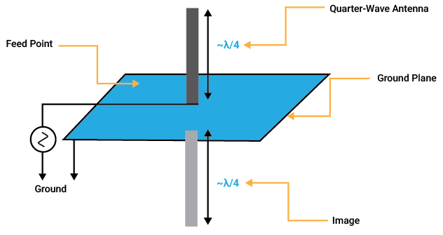
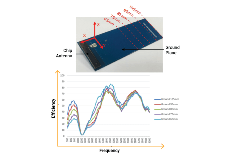
The counterpoise shall be at least λ/4 units in length and width. The effect of various ground plane dimensions is shown in the image below using an example of a chip antenna implementation.
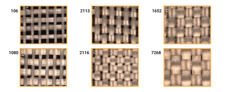
Furthermore, the PCB material also influences the antenna system impedance. Especially for FR4 type substrates, which are also dependent on the weaving pattern that causes changes in the dielectric constant of the material as per the tightness of the weave and can cause local impedance discontinuities due to changes in parasitic capacitance. For a PCB trace antenna implementation, it is imperative for a designer to follow the antenna design guideline and the antenna manufacturer’s recommendations closely with respect to trace width, layer stack-up, counterpoise dimensions, PCB material and material weave pattern to achieve optimum results while implementing a trace or a chip antenna. The antenna system impedance is also affected by other circuit components surrounding it and the product enclosure material and shall be taken into account.
Debugging Antenna using Vector Network Analyzer (VNA)
An impedance mismatch can be debugged using a Vector Network Analyzer (VNA). The VNA measures at the plane of calibration by default and is required to be calibrated before the measurement can be taken. For matching impedance between antenna and the RF chip, return loss (RL) also known as the S11 parameter needs to be measured.
Let’s understand the methods of Calibration of Vector Network Analyzer (VNA)
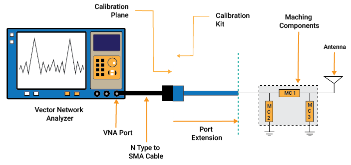
Most VNAs come with N-type connectors as their ports. The first step to debug any antenna system is to calibrate the VNA at the calibration plane by using an N-type to SMA cable and various(open, short and 50Ω) calibration standards. The VNA must be connected to the antenna system such that the matching network is also included in the measurement process. This can be done by mounting a 0Ω series resistor at “MC1” and using a suitable cable which is termed as “Port Extension”. It is necessary that the port extension is of a known length and a known velocity factor since this data needs to be fed into the VNA in order to compensate for the extra length and the impedance that the port extension adds to the system during the measurement. Furthermore, the port extension should be selected such that its characteristic impedance matches the target system impedance.
Another method of calibrating a VNA is to create a Short/Open/Load (SOL) condition on the PCB itself using the matching component pads. This does not require a port extension to be applied. As per the board implementation, a suitable method out of the two shall be chosen.
Impedance Matching using Smith Chart
The VNA provides the impedance of the antenna system in the complex R+jX Ω form where R is the real part of impedance arising due to pure resistance and X is the complex part of the impedance arising due to reactance. After the complex impedance of the antenna system is obtained, it can be plotted on a “Smith Chart” in order to determine the values and topology of matching components required. Nowadays, this can be done easily using a program such as “SimSmith”.
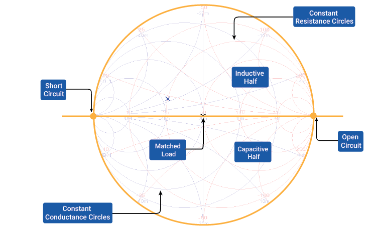
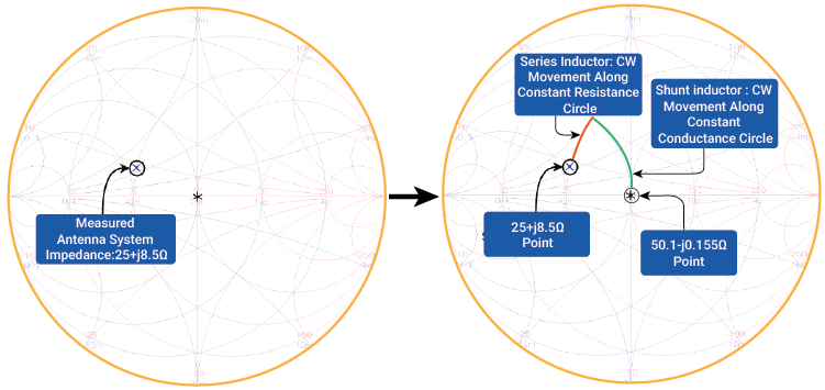
Feeding the complex impedance of the antenna system into SimSmith will result in a point being plotted on the corresponding point on the smith chart. As shown in the image above, the complex impedance of the antenna system can lie in either inductive or capacitive halves of the smith chart. Determination of the matching network components to match the antenna system to the target matched load is done by utilization of a few key points:
- A series inductor moves the plotted complex impedance point in a clockwise fashion along the constant resistance circle
- A series capacitor moves the plotted complex impedance point in an anticlockwise fashion along the constant resistance circle
- A shunt inductor moves the plotted complex impedance point in anticlockwise fashion along the constant circle
- A shunt capacitor moves the plotted complex impedance point in a clockwise fashion along the constant conductance circle
- Multiple components or a combination of multiple components might be required in series or shunt configuration to match the targeted impedance
- Use of series inductor and shunt capacitor is preferable since increasing the component values of both causes the plotted impedance point to move further along the locus of the constant resistance/conductance circle. This is advantageous since very low values of either inductor or capacitor cannot be realized practically
- Using a single matching network often causes degradation of system bandwidth, multiple stages of the matching networks can be used to realize proper matching and optimum bandwidth
As an example, the image below shows the matching of an antenna system with a complex impedance of 25+j8.5Ω to the target impedance of 50Ω using a series inductor and a shunt capacitor.
As complicated as the impedance matching seems, it ensures the optimum performance of any wireless product without which an antenna can become a bottleneck in the product performance.
About VOLANSYS
VOLANSYS has vast experience in designing and developing the hardware of complex, faster, reliable, and efficient solutions. Our RF antenna design services extend through design specification, antenna prototyping, impedance matching, network analysis, smith chart, optimization and verification of the selected antenna, and many more. Our experts ensure impedance matching and reduce power losses between the antenna and RF transmitter.
To know more about our work on RF antenna design, read our hardware engineering success stories.

About the Author: Sarth Dave
Sarth is working with Volansys as a Senior Engineer. He has 5+ years of experience in the hardware and embedded field and is involved in system architecture, design and development, testing, certification and manufacturing readiness of a product.

