


Designing a high-speed board is an essential part of embedded applications. Nowadays, a printed circuit board (PCB) is designed in such a way that it should automatically meet the requirements of advanced solutions. That is the biggest reason why high speed and high-frequency PCB design has become an important topic for hardware engineers.
The right approach in hardware design is becoming a necessity to be competent in the product design service to achieve the defined project timeline and cost for the product companies. While designing high-speed boards having interfaces like PCI Express, SATA, and LPDDR4, it is even more challenging to achieve the first right reliable design without in-depth knowledge and experience in high-speed designs.
When we speak about high-speed board designs, there are many areas to work on during the hardware design life cycle starting from architecture design such as component selection, interface timing and DC characteristic analysis, schematic design, required stack up design, layout design, SI analysis, PI analysis and many more. To highlight the high-speed design practices, below we have discussed initial two important steps in detail:
Floor Planning Strategy
Floor planning is a visual diagram that visualizes the placement of all the interconnecting sub-sections on the board. The layout routing without proper floor planning may lead to the increased size of the PCB, parasitic effects, routing congestion, EMI issues, more number of layers requirement in layer stack up, etc. Usually, floor planning is nearly owned for estimating the PCB size, isolating the analog-digital, RF subsections on the PCB, and finalizing the placement of the electromechanical components based on the product enclosure design.
The second level of floor planning is required for the high-speed board designs to avoid rework during the PCB layout as well as increased time and cost of the design at a later stage. One of the good practices for the placement of interconnecting modules is to divide the PCB real estate into multiple blocks and then decide in which block the interconnecting module can best fit based on the shortest possible interconnection between driver and receiver or transceivers. This will help in identifying the routing directions and required layers in the PCB stack-up.
Let’s understand important parameters for optimized placement on the board:
- Select the small package-sized component for high-speed boards to reduce impedance mismatch and parasitics, inductance and capacitance, on the high-speed transmission lines. Beware, there may be yield issues with a smaller component package. Take decisions by consulting the assembly vendor based on their capabilities
- Begin the placement with high pin count components and electromechanical connectors
- Group the components into logical sub-sections and follow the schematic logic flow for the component or logical sub-section placement
PCB Layer Stack-up
- Determining the Number of Layers Required: The signal layers depend on the signal integrity requirements like low crosstalk, low pitch components, high pin count components such as BGAs, fixed PCB size, etc. The power and ground layer count depends on the power distribution, low EMI, and signal return path requirement in the high-speed design, reducing the DC voltage drop in the power rails and increasing the power integrity.
- Layers Arrangement in the Layer Stack-up: Once the number of signals, power, and ground layers are determined, the next step is to arrange them sequentially. There are few rules we need to follow in the layer stack-up arrangement are listed below:
- Power and ground planes should be close to each other for good inter plan capacitance
| Layer | Name | Material | Thickness | Constant |
| 11 | Dielectric 5 | FR4 | 4.49mil | 4.42 |
| 5 | L5_GND-2 | Copper | 0.71mil | |
| 13 | Dielectric 6 | 4.93mil | 4.32 | |
| 14 | Dielectric 7 | 4.93mil | 4.32 | |
| 15 | L6_PWR-1 | Copper | 0.71mil | |
| 16 | Dielectric 8 | FR4 | 4.49mil | 4.42 |
| 17 | L7_PWR-2 | Copper | 0.71mil | |
| 18 | Dielectric 9 | 4.93mil | 4.32 | |
| 19 | Dielectric 10 | 4.93mil | 4.32 | |
| 20 | L8_GND-3 | Copper | 0.71mil | |
| 21 | Dielectric 11 | FR4 | 4.49mil | 4.42 |
| Layer | Name | Material | Thickness | Constant |
| Dielectric 5 | FR4 | 4.49mil | 4.42 | |
| 5 | L5_GND-2 | Copper | 0.71mil | |
| Dielectric 6 | 4.93mil | 4.32 | ||
| 6 | L6_PWR-1 | Copper | 0.71mil | |
| Dielectric 7 | FR4 | 14.35mil | 4.42 | |
| 7 | L7_PWR-2 | Copper | 0.71mil | |
| Dielectric 8 | 4.93mil | 4.32 | ||
| 8 | L8_GND-3 | Copper | 0.71mil | |
| Dielectric 9 | FR4 | 4.49mil | 4.42 |
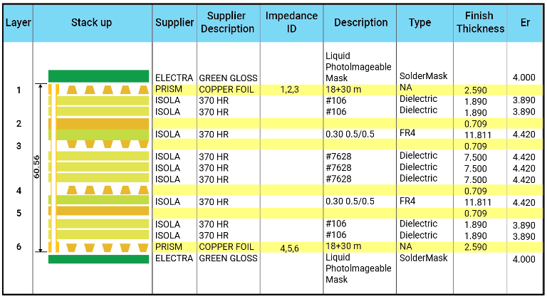
- Avoid two signal layers adjacent to each other. If not possible then make sure to have low prepreg thickness between signal layer to reference ground layer and high core laminate thickness between two signal layers as shown in the image below
| Layer | Name | Material | Thickness | Constant |
| 5 | L2_GND-1 | Copper | 0.70mil | |
| 6 | Dielectric 2 | FR4 | 4.00mil | 4.17 |
| 7 | L3_SIG-1 | Copper | 0.70mil | |
| 8 | Dielectric 3 | 6.12mil | 3.82 | |
| 9 | L4_SIG-2 | Copper | 0.70mil | |
| 10 | Dielectric 5 | FR4 | 4.00mil | 4.17 |
| 11 | L5_GND-2 | Copper | 0.70mil |
- Build symmetric or balanced stack-up from the center towards the top and bottom
- Add possible ground layers in the stack-up to reduce the common-mode radiation from the high-speed signals
Determining the Material Type: The PCB is made up of four different types of materials, i.e., silk screen printing material, solder mask material, copper, and substrate. The substrate material which influences the high-speed design parameters like, impedance and signals integrity, is FR4 in most common applications. The high-speed board components dissipate more heat than ordinary boards due to fast clock rates and data transfers which conductively spreads to PCB as well. The designers can select the moderate or high Tg, glass transition temperature, FR4 material for long-term operational reliability. The Tg is a temperature where the PCB substrate starts becoming mechanically unstable. The FR4 is suitable for the application having <5GHz clock rates. High-speed boards beyond 5GHz require other materials to be used like Nelco and Megtron. For the frequency above 56GHz certainly, microwave frequencies need Rozer material to be used in stack-up
After defining the layer stack-up, now it’s a time where the designers should start involving their PCB fabricator or contract manufacturer to get the practical possible stack-up based on the material availability, substrate thickness, and required signal impedance. To achieve the desired impedance, the PCB fabricators are adjusting the stack-up dielectric thickness during the PCB manufacturing. One can check with the manufacturer and ensure the verified achieved impedance during manufacturing is within tolerance for single-ended and differential signals.
If you are ready to design your own high-speed board or want to connect with one of our experts for consultation, feel free to contact us.

About the Author: Ritesh Patel
Ritesh works with VOLANSYS Technologies as a Senior Technical Lead and looks after his team for embedded product design. He has around 9+ years of demonstrative product engineering experience in various domains like IoT, Consumer, Industrial, and Automotive which includes end-to-end solutions from involvement in product conceptualization, architecture design, hardware design and development, product certifications to the manufacturing transfers.

