


In the product design lifecycle, mass manufacturing is done at the final stage of product release. There are several factors such as good design, minimum PCB assembly re-operations & iterations, less material overhead and labor cost to consider in this stage to manufacture valued products for OEMs and enterprises.
To achieve this, Design for Manufacturability (DFM) and Design for Assembly (DFA) techniques are widely used in an integrated and controlled manner. Sometimes, also called DFMA (design for manufacturing & assembly), which is used to minimize product cost & time through design and process improvements.
In manufacturing services, DFM is the process used for ease of manufacturing, while DFA is the method of design used for ease of assembly in product design. It is applicable to PCB fabrication or PCB assembly or product assembly. Good DFMA practices can accelerate the manufacturing process and provide an added advantage of reduced cost, material wastage, increased yield from available resources and ultimately save time and scale up the production.
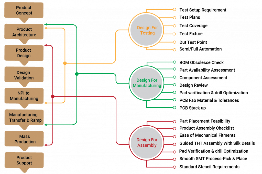
DFT is the method of design to ensure PCBA level operational & functional testing facilitated by test points on the board. Once the physical manufacturing process is finished, DFT helps to validate the board’s assembly and ensure product hardware is manufactured defect-free.
In this article, we would take a closer look at the DFA/DFT/DFM guidelines, and their importance to production processes. Let’s get right on it.
DFM Guidelines
- Eliminate expensive, complex or unnecessary features for easy manufacturing
- Avoid tight tolerances, accommodate within manufacturing process capabilities (e.g. PCB stackups, trace width-spacing, thickness & via/hole/cutout toolings)
- PCB panelization is very important factor in PCB fabrication cost
- Good to avoid parts with sharp edges & points, better to use radial chamfering
- Try to avoid bulky parts in design to reduce fatigue and lifting challenges
- Avoid rigid-flex PCB design if not mandatory
- Avoid uneven pads & irregular shapes in footprints for better etching
- Minimize solder-mask offsets for sufficient solder-joints in reflow process
- Use more thermal vias (instead of bigger Via holes)
DFA Guidelines
- Minimize the number of part count & types of parts to reduce inventory handling, sourcing, stock and assembly time
- Use parts with self-locating/aligning features & which can’t be installed incorrectly
- Design parts with self-fastening features to support mechanical challenges
- Use single side PCB for part placement
- Follow the ‘Top-Down’ assemblies approach for gravity advantage
- Do product design considering different parameters for a smooth assembly process like system partitioning, interconnection type and its assembly inside product, size and a package of parts, a minimum distance between assembly parts, etc.
- Provide parts enough clearance from PCB edges and also maintain minimum clearance between two components in a dense board considering the assembly process capability
- Arrange similar components symmetrically for easy installation
- Take care of mating connectors, cable orientation/height and area requirement
- Avoid using parts that are tangled prone & difficult to pick up/handle during assembly
- Avoid uneven pads & irregularities in footprint pads as it would require manual touch-up after surface mount technology to achieve optimum solderability
- Big size thermal vias impact GND-pad solderability, so use via tenting/filling/plugging (generally resin fill or conductive/non-conductive material)
DFT Guidelines
- Implement product testability starting from the development or prototype stage
- Cover all critical signals for testability
- Should have single side test points for added advantage on test set-up with Bed of Nail (BoN)
- Consider test points size and minimum pitch of test points right from the design phase to achieve Bed-of-nail (BoN) set-up within capabilities
- Ensure low skew between TAP signals (e.g xJTAG) & Buffer TAP signals with voltage level separations (inside TestFixture wiring)
- Consider testing multi-board panels as one unit
- Test points should have enough clearance to pad/component/PCB edge
- For full ICT (In-circuit test) coverage, every net of design should have test points
- Emphasize Test-flow to isolate issues related to component failures and manufacturing errors
- Choose correct spring-loaded probes (pins) to facilitate a proper electrical connection
- Avoid bulky & heightened components to use Flying probe testing
- Testing time per unit is crucial & target should be to achieve as minimum as possible
- Test automation should be driven from ease of testing, limited test-points, simple system feedback mechanicals
- Design test fixtures to cover functional validation either by semi OR full automation
VOLANSYS helps OEMs whether startups or scale ups to timely market their product and reduce costs with Hardware engineering services, mechanical design engineering services, and electronics manufacturing services. The VOLANSYS team has in-depth knowledge of executing DFMA & DFT processes in various stages of the product development cycle, they are aware about necessary design guidelines to ascertain all flaws of Product Manufacturability, Assembly, Testing and more. This makes a vast difference in product quality and optimized hardware design facilitating all supported product features.
Our Domain experts align with client’s product requirements following integrated practices right from architectural structure, part selection, hardware/firmware design/development towards Manufacturing transfer, etc. Our Manufacturing team is experienced in various product’s manufacturing with controlled processes to ascertain quality at reduced cost & higher yield records. VOLANSYS would facilitate companies to get priority access to our partner PCB Fabrication Labs, PCB Assembly Houses and in-house Product Testing & Finished assembly executed by a well-trained manufacturing team. To know more about our work read our success stories.
About the Authors:

Bimal Makwana
Bimal Makwana works with VOLANSYS Technologies as Principal Engineer and looks after Embedded Hardware Design and end to end solutioning. Bimal has a rich experience of around 7+ years in various domains of product development which includes from product concept, system architecture design to final certification that brings greater value to our clients to implement a one-stop solution.

Jay Patel
Jay Patel is associated with VOLANSYS Technologies as Principal Engineer for more than 4 years. He has rich experience working in Embedded Hardware domain involving product design right from concept/feasibility, system architecture, PoC/MVP, final product certification to mass production transfers. He also supports field trials/deployments of consumer and industrial products for our clients.

